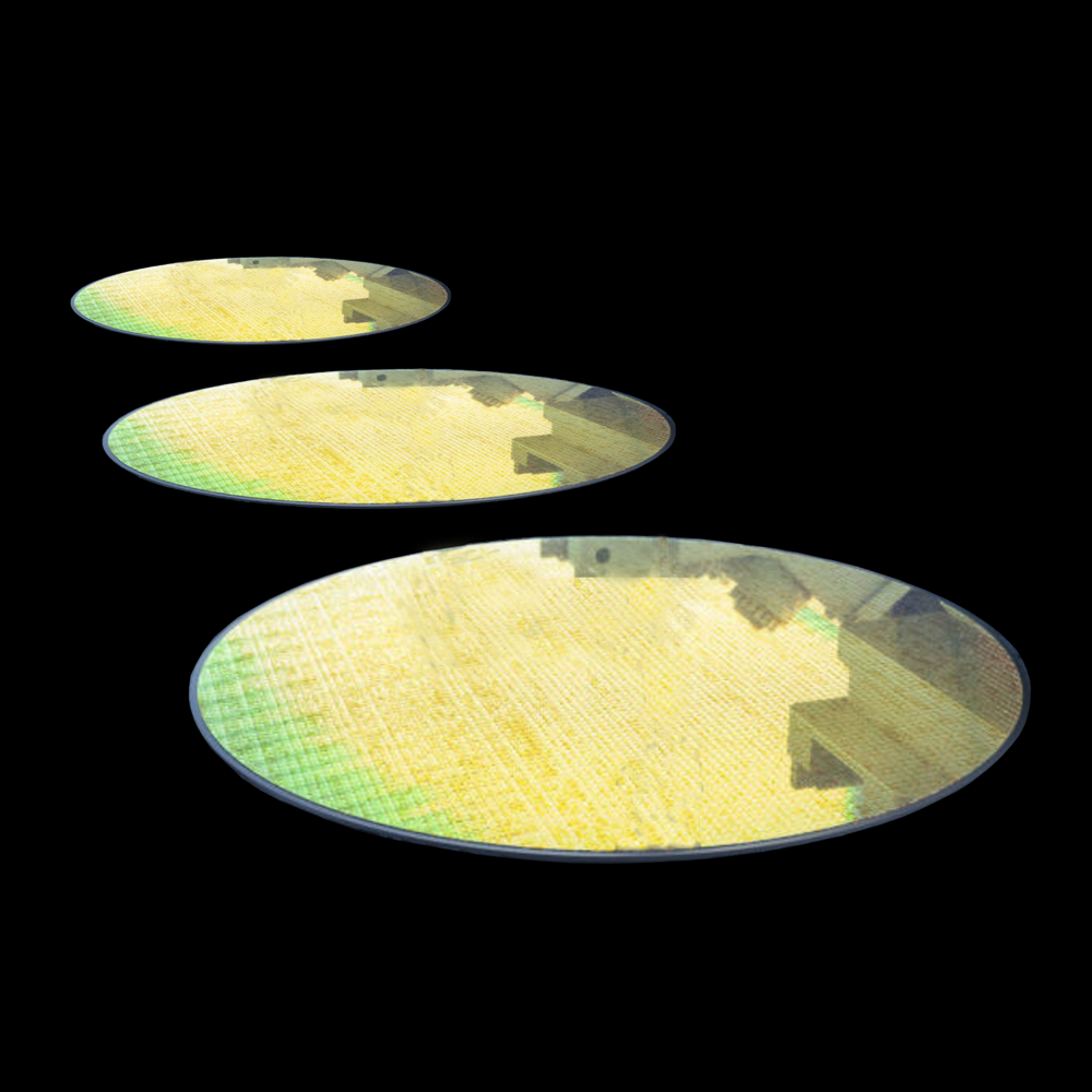
Wafers serve as the foundation for semiconductor device fabrication. They provide the surface on which integrated circuits are patterned, enabling mass production of microelectronics for computing, communications, and sensing.

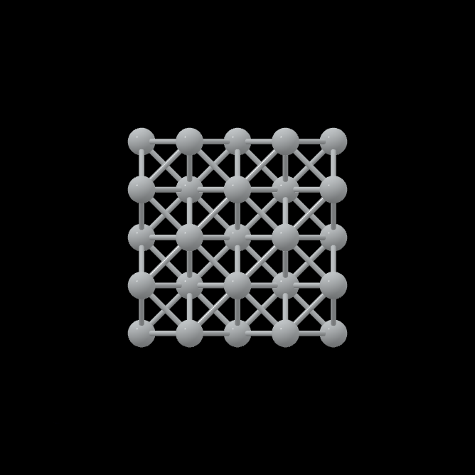
Silicon wafers are the most common semiconductor substrate, valued for their purity, crystalline structure, and scalability. They enable cost-effective chip manufacturing for processors, memory, and sensors.
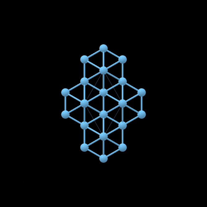
Diamond substrates offer exceptional thermal conductivity, mechanical strength, and wide band gap properties, making them ideal for high-power, high-frequency, and heat-intensive semiconductor applications.

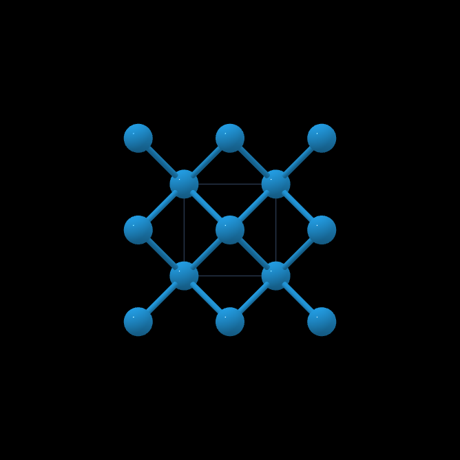
Silicon dioxide, often deposited from TEOS precursors, is widely used for insulating layers, passivation, and dielectric films, ensuring device stability, electrical isolation, and reliable performance.
Anti-Reflective Layers (ARL) reduce light reflection during lithography, improving critical dimension control and pattern fidelity. They are essential for precision manufacturing at advanced semiconductor nodes.
.png)
Aluminum is commonly used for interconnects due to its conductivity and ease of deposition. It remains important in certain device architectures despite the rise of copper and other advanced materials.

Molybdenum provides durability, high melting point, and conductivity. It is often used in thin films, electrodes, and contact layers in semiconductors, supporting device stability and performance.
Silicon nitride films are used as dielectric layers, diffusion barriers, and passivation. Their excellent mechanical strength and chemical resistance make them vital for device protection.
.png)
Silicon oxynitride combines properties of SiO2 and SiN, enabling tailored dielectric performance. It improves reliability in gate stacks and optical applications within semiconductor devices.
.png)
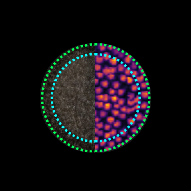
Amorphous silicon is versatile, used in thin-film transistors, solar cells, and sensors. Its ease of deposition on large substrates supports applications beyond traditional integrated circuits.
.png)
GaN is a wide-bandgap semiconductor material enabling high-power, high-frequency devices. It’s crucial for efficient power electronics, RF components, and next-generation optoelectronics.
.png)
Indium gallium oxide (IGO) is an emerging transparent conductive material used in thin-film transistors and displays. It offers high mobility, transparency, and stability for advanced electronics.
.png)
Barrier coatings protect packaged products from oxygen, moisture, and contaminants. They extend shelf life, maintain quality, and support sustainable packaging solutions across food, pharma, and electronics.

Polymer films serve as lightweight, flexible substrates for packaging. They provide strength, printability, and barrier compatibility, supporting multilayer structures for food, medical, and industrial applications.
Silicon dioxide combined with niobium oxide enhances barrier performance by reducing permeability. These coatings are used for advanced packaging requiring durability, optical clarity, and chemical stability.
Silicon dioxide is widely used as a transparent barrier and protective layer. In packaging, it provides resistance to oxygen and moisture, ensuring product stability without compromising clarity.
Packaging materials are classified as polymers, oxides, or composites based on their chemistry. Each class contributes specific barrier, mechanical, or optical properties to meet diverse application needs.
Genomics devices enable sequencing, analysis, and interpretation of genetic material. They support precision medicine, diagnostics, and biomedical research through high-throughput and reliable performance.
Silicon with polymer coatings combines electrical performance and biocompatibility. These hybrid layers are used in biochips and sensors for durability and controlled interactions with samples.
Industrial glass windows are engineered for durability, optical clarity, and energy performance. They are used in buildings, vehicles, and specialty applications requiring controlled light and heat transmission.
Low-emissivity (LowE) coatings with tin oxide layers reduce heat transfer while maintaining visibility. They improve energy efficiency, solar control, and comfort in architectural and industrial glass.
Chemical classification defines glass and coating materials by composition, such as oxides or metals. This ensures performance predictability and guides application-specific material selection.
The piezoelectric coefficient measures how effectively a material converts electrical energy into mechanical displacement. Higher coefficients improve haptic sensitivity and performance.
Nickel alloys offer exceptional strength, oxidation resistance, and thermal stability. They are the primary substrate for turbine blades, ensuring performance in high-temperature aerospace environments.
Thermal barrier coatings insulate turbine blades from extreme heat. Typically ceramic-based, they extend component life, improve efficiency, and protect against oxidation and corrosion.
Microstructure refers to the grain size, phases, and defects within a material. Controlled microstructures improve creep resistance, fatigue strength, and coating performance in aerospace parts.
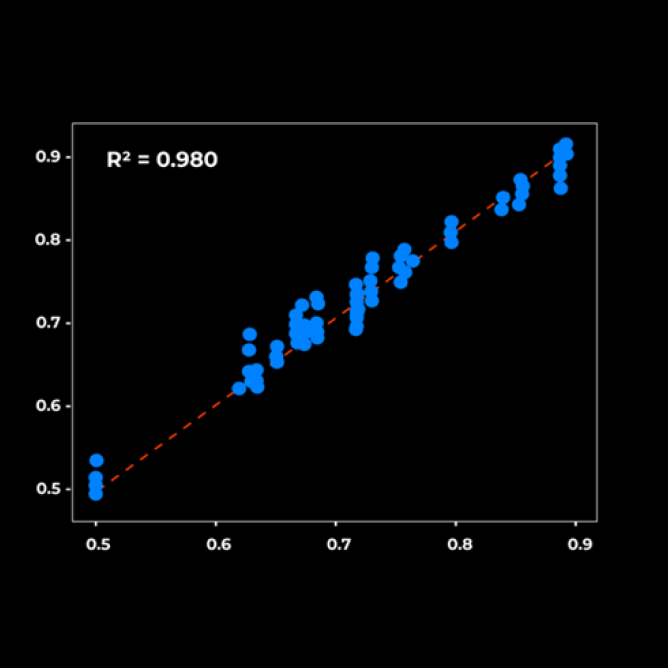
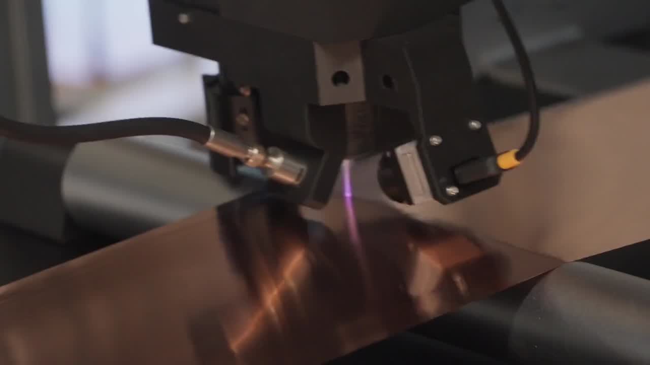
Real-time, non-destructive material analysis using cold atmospheric plasma and AI-driven insights


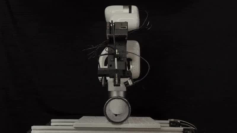
Our benchtop, general purpose system for fast, non-destructive material analysis
Stage Size
Optimized for flat samples and precision surface analysis up to 150mm x 180mm
Flat Samples
Ideal for films, wafers, and coated surfaces requiring high-resolution mapping.
Stable
Secures samples firmly to eliminate vibration and ensure measurement stability.
Environment
Operating conditions between 20–45°C, <1% RH, Dew Point -40°C to -80°C
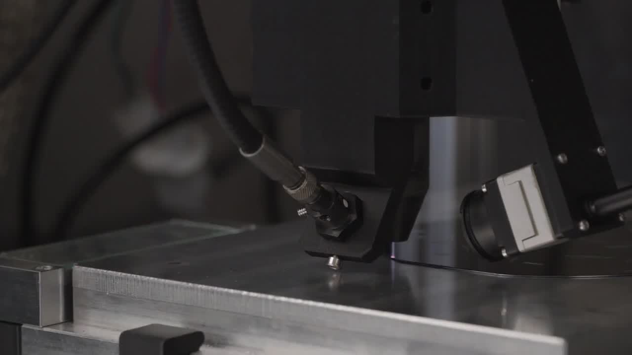
Robot-arm mounted PlasmaSens for real-time piece-to-piece inspection, inline and offline
Sample Size
Supports a wide range of part sizes for inline or offline inspection.
Full Motion
Enables precise inspection of complex geometries and varied orientations.
Raw Data Signals
Rich, multidimensional data for comprehensive material analysis.
AI-Based
Delivers immediate pass/fail feedback and enables predictive quality control.
PlasmaSens for continuous, real-time monitoring in high-throughput production
Speed
Supports continuous high-throughput inspection in production environments.
Compatibility
Flexible integration with a wide range of roll-based substrates up to 1.5m width.
Wide
Cathodes, NMP solvent w/ binder PVDF, PE separators, AlOx coatings, Anodes, binder.
Environment
Operating conditions between 20–45°C, <1% RH, Dew Point -40°C to -80°C


SirenOpt Secures Strategic Investment to Accelerate Commercialization of Its PlasmaSens Manufacturing Intelligence Platform for Factory Applications
Read More